ACT88760
5 V PMIC with 7 High Current Bucks, 6 LDOs and 10 GPIOs
The full Product Data Sheet linked below is accessible through the Document Request form.
For the Product Data Sheet Brief, please see the Documents tab.

Key Features
- 2.6 - 5.8V input voltage range
- 0.5 - 3.8V output voltage range
- Bucks 1 & 2: 4A bucks. Can operate in dual phase mode (8A)
- Bucks 3 & 4: 3A bucks. Can operate in dual phase (6A)
- Bucks 5 &6: 2A bucks
- Buck 7 :4A, optimized for high efficiency with low VOUT (<1V)
- LDO 1& 2: 800mA, can accept low input voltage of 1V, high PSRR (> 70dB)
- LDO 3& 4: 400mA LDOs
- LDO 5& 6: 400mA LDOs or configured as Load switches (up to 1.5A and low 25m Ohm insertion on-resistance)
- 10 configurable GPIOs
| Mouser | 2943 | Buy Online > | |
| RELL | 100 | Buy Online > | |
| RFMW | 18 | Buy Online > |
The ACT88760 PMIC is an integrated ActiveCiPSTM power management integrated circuit. It powers a wide range of processors , including Solid-state drive Applications, Video and AI processors, FPGA's and computer vision. The ACT88760 is optimized for mid power applications like enterprise SSDs, video cameras, AR/VR devices, connected home devices, FPGAs, LPDDR5 applications etc. It is highly flexible and can be reconfigured via I2C for multiple applications without the need for PCB changes. The low external component count and high configurability significantly speeds time to market. Examples of configurable options include output voltage as low as 0.5V, startup time, slew rate, system level sequencing, switching frequency, sleep modes, operating modes etc.
The core of the device includes seven high efficiency switching regulators, six linear regulators – LDOs or load switches. Two LDOs - LDO5 & 6 can also be configured as a load switches (LSW) and there are ten GPIOs pins that are configurable and used for a variety of system functions. The ACT88760 is designed to work with a single lithium ion or lithium polymer batteries with an input voltage up to 5.5V. It works with input voltages as low as 2.6V and can step down to output voltages as low as 0.5V. The Bucks can work in dual phase for higher power. LDO5 and 6 can function as load switches with typical RDSON < 25m and up to 1.5A of output current or as LDOs up to 400mA. LDO 1 & 2 are designed for high PSRR 70dB and provide up to 800mA of output current.
Typical Applications
- Solid State Drives
- FPGA
- Computer Vision
- Portable Audio / Video
Product Categories
Application Categories
| Application Processors | General purpose |
| Battery Charger | No |
| Input Voltage(V) | 2.7 to 5.5 |
| Buck Converters | 7 |
| Bucks Configurable as Load Switch | 0 |
| Boost Converters | 0 |
| Buck-Boost Converters | 0 |
| LDO Regulators | 6 |
| LDOs Configurable as Load Switch | 2 (LDO 5&6), with 1.5A max current |
| Interface | I2C |
| Package Type | WLCSP, 81-pin |
| Package(mm) | 3.85 x 3.85 |
| RoHS | Yes |
| Lead Free | Yes |
| Halogen Free | Yes |
| ITAR Restricted | No |
| ECCN | EAR99 |
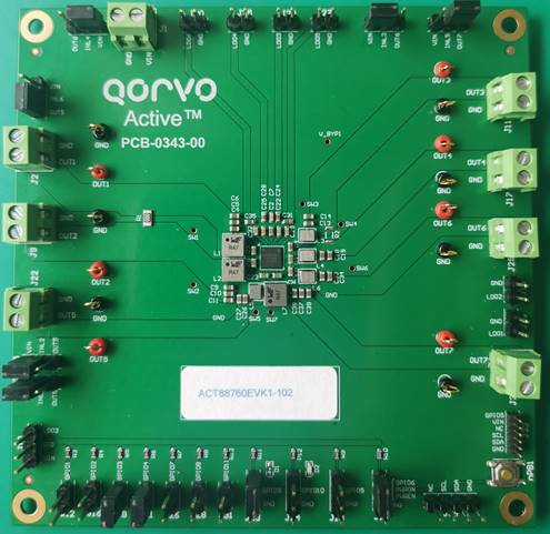 ACT88760EVK-102.E2 Evaluation Kit
ACT88760EVK-102.E2 Evaluation Tool User Guide
The Evaluation Tool Users Guide describes the characteristics and operation of the Qorvo ACT88760EVK-102.E2 evaluation kit (EVK). It provides setup and operation instructions, schematic, layout, BOM, and test data.
To communicate with the EVK a USB Dongle and a Graphical User Interface (GUI) is provided.
This EVK demonstrates the ACT88760-102 ActivePMU power management IC.
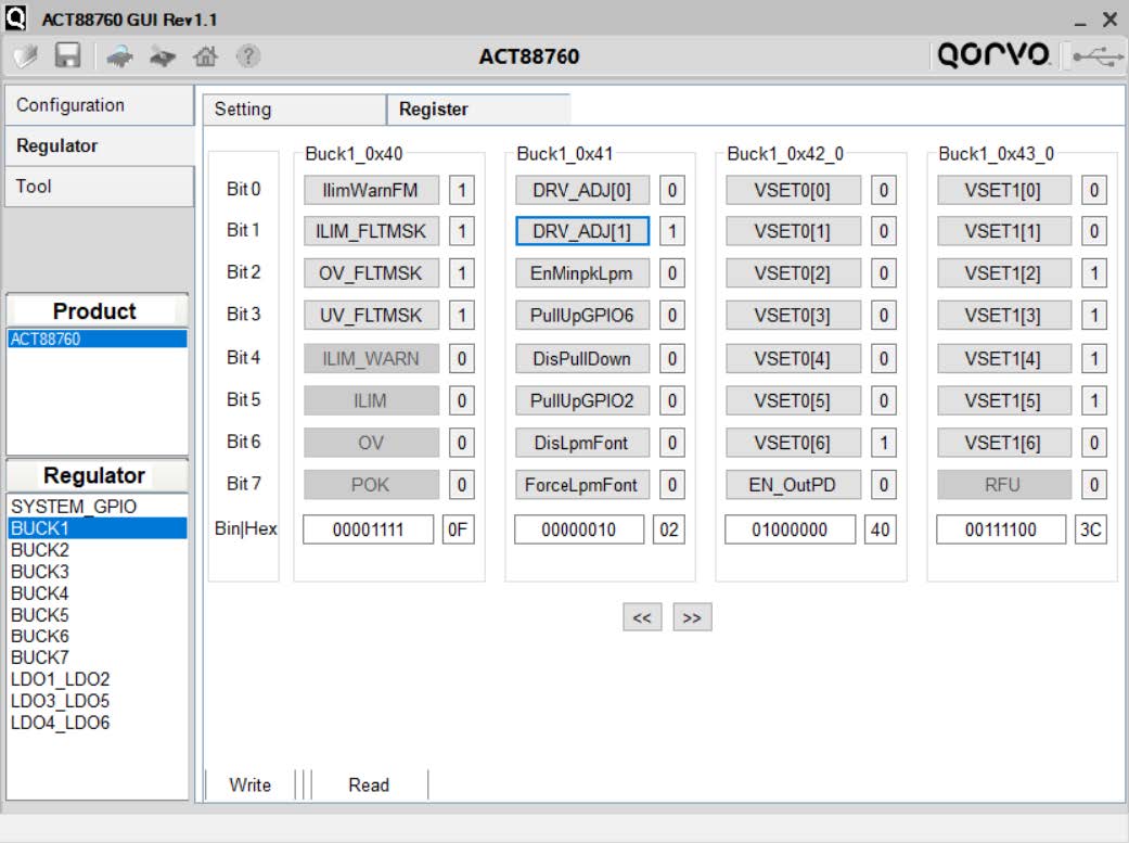 ACT88760 GUI
The ACT88760 EVK Graphical User Interface (GUI) is packaged in a ZIP file that includes the software and all necessary drivers to communicate with the ACT88760 Evaluation Tool, as well as all descriptions how to use the tool.