Power Solutions for Phased Radar
September 11, 2023
Technology is always evolving. Gallium Nitride (GaN) technology, along with power management integrated circuitry (PMIC) in phased array radar systems, is part of this evolution. GaN entered the market some time ago with differences in operational methodology but with the key advantage of higher power, wider bandwidth and high breakdown voltage performance over previous generational technologies. Making it a good fit for radar applications.
One such operational difference was its biasing sequence. GaN is a depletion mode Field Effect Transistor (FET) – needing a negative Gate voltage during operation. This negative Gate voltage, sometimes called “pinch-off,” must be applied prior to increasing the positive Drain voltage. If this bias sequence is not properly done, the GaN device can be damaged. But technological evolution has made this task easier using PMICs.
In the following paragraphs, we explore how PMICs can be used to make the design of a phased array radar system easier. While at the same time, the implementation of these PMICs can help designers create a more optimized, robust and self-calibrating radar system with superior performance.
A Look at the Radar System Challenges
GaN's performance far outweighs any design challenges an engineer faces when using it in their phased array radar system. The ability to attain higher efficiencies, have high-power system capabilities, high-device breakdown voltage characteristics, wide bandwidth, and not to mention its high thermal properties – are all compelling when creating a radar system.
Take a Deeper Dive
Qorvo's Phased Array Radar Power Solution with Bias Autocalibration.
Learn More
So, let's review some hurdles using GaN as well as some power supply challenges facing engineers in phased array radar design...and then show how the introduction of powerful and small integrated PMICs allows us to jump these hurdles.
A look at the GaN RF Front End design hurdles in a phased array radar system:
- Controlling the negative Gate pinch-off and turn-on voltage of the GaN PA.
- Controlling the RF Front-End Drain bias current of the GaN PA.
- Precisely detecting, monitoring and optimally setting the Drain bias current or current Drain quiescent (IDQ).
- Implementing self-calibration for the entire RF Front-End to attain a uniform performance.
- The GaN Gate voltage must be swept from -5 Volts to -2.5 Volts while monitoring its Drain voltage.
- Increase the RF Front-End system protections
- A procedure enabling all the above each time the system is powered up – providing auto-tuning under conditions such as aging or temperature fluctuations.
From a power supply perspective, there are additional hurdles – those being:
- The need for large, expensive power bricks to address the heavy pulse load at the transmit module.
- Large gauge cabling to deliver the high current and voltage to the transmit module.
- Large bulky aluminum capacitors to generate high wattage power brick performance.
- High RDS (ON) FETs, used as a drain switch to power the GaN PA on and off.
- Large Gate bias control circuitry to provide Gate control.
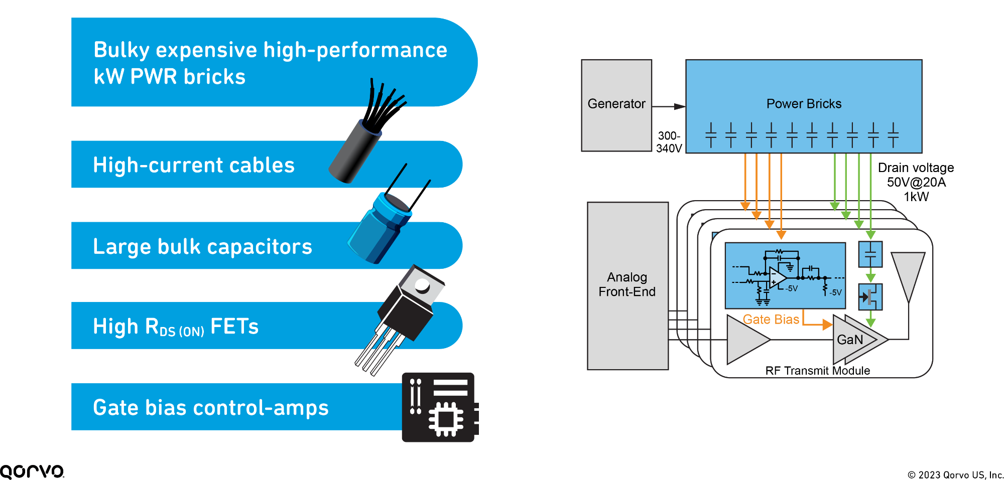
Figure 1. The design hurdles in a phased array radar system.
To date, the above hurdles have been difficult for engineers to navigate and made the design process longer and more cumbersome. But by using PMICs, the design process can be shortened, and the overall phased array radar system is made more efficient, smaller and reliable.
In the following paragraphs, we will explain how using PMICs in a phased array radar system addresses the above bullets.
A Deep Dive into PMICs for Phased Array Radars
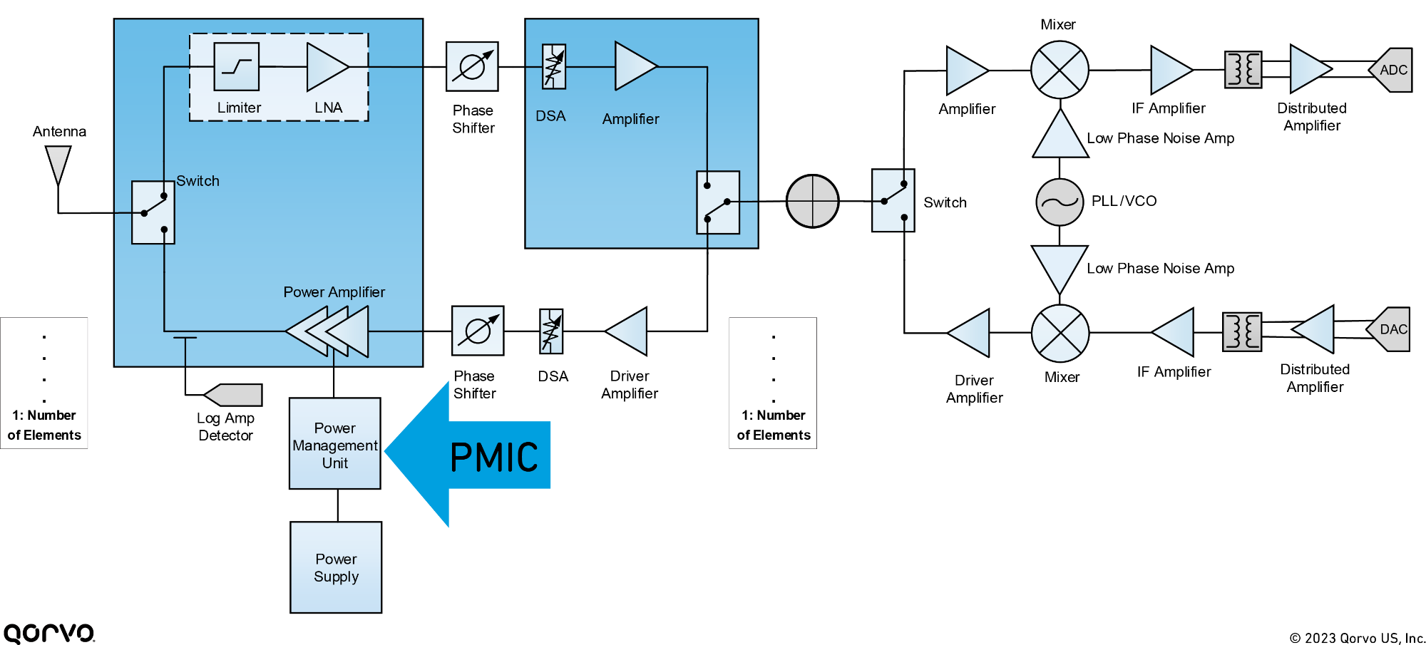
Let's first look at how the overall phased array radar system is powered. Land, sea and airborne radar equipment are typically powered from A power derived from diesel generators or high-voltage DC-powered battery banks. These AC-DC and high-voltage DC-DC power supplies are required to deliver a well-regulated low voltage DC voltage rail from which the PA can be reliably run. Qorvo's SiC FETs and Schottky diodes, as shown in Figure 3, enable designers to build robust, efficient and compact power supplies for phased array radar systems.
As shown in Figure 3, a Qorvo phased array radar power supply, the silicon carbide (SiC) FET devices provide a 10-55 Volt constant DC rail voltage powering both the PMICs and RF systems. After the power supply, a two-stage supply PMIC controller is used to control the DC rail voltage – providing a low noise fast responding DC supply rail to the PA. Additionally, this PMIC design (the ACT43950 and ACT43850) removes the need for the large bulky power brick, aluminum capacitors, large FETs and Gate bias controller. This system design supports RF GaN devices with Voltage ranges between 20 to 55 Volts.
The addition of the PMIC (ACT43750) controls the GaN PA, providing a fully reliable configurable system that both monitors and controls the phased array radar PA. Note – the ACT43750 can also be used independently if your system design already has the voltage rails implemented. In this case, the ACT43750 and switch (GaN or Si) are added. A system design using only the ACT43750 supports a 10 to 55 Volt DC constant rail for the GaN device in the RF system. However, it must be understood that without the addition of the ACT43950 and ACT43850, your design will require larger power components and wiring, as outlined above.
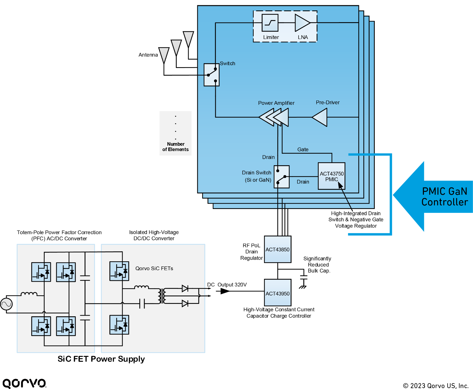
Figure 3. Phased array radar PMIC and power supply.
Let's explore the above Figure PMIC resolution in detail.
First, let us look at the power supply PMIC. The ACT43950 works as a transmission phase transient shock averaging block, which replaces bulky power line filters from the DC rail source. The ACT43850 or RF Point of Load (RFPoL) provides a low noise, fast responding DC supply for the RF PA Drain nodes. These two ICs significantly reduce system size by removing the need for bulky capacitors and large gauge wires at the PA Drain nodes. Moreover, they remove the need for large Gate switch FETs and the Gate bias circuitry.
For the GaN controller PMIC section, the ACT43750 regulates and controls a GaN PA Gate at low noise for RF PA sequencing and protection. It further offers an automated RF PA Gate voltage calibration to control the Gate voltage to the IDQ bias point. The ACT43750 has two power management blocks. The first block controls the Drain switch for the RF PA of 20 V to 55 V. The other is an ultra-low noise inverting buck (step-down) DC-DC regulator with integrated FETs and programmable voltage reference. (some GaN PAs suited for this voltage range are – QPA2612, QPA2237, QPM0106 and QPD1017 – others are located here). Not only does this device control the power side of the GaN device, but it also provides auto-tuning self-calibration for conditions such as aging or temperature fluctuations. This self-calibration happens instantaneously while in operation. For lower-power PMIC controllers, the ACT41000 can be substituted. We will dig more into that in a follow-up blog post.
This bundled solution of GaN PAs, PMICs and SiC FETs gives engineers the flexibility to optimize their phased array radar system performance and design. With the aid of the three-stage PMICs, engineers can configure the GaN bias point autocalibration for each PA without changing the board design to match the PA. This helps engineers speed their design and provides the needed flexibility to get them to market faster with a small footprint solution.
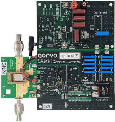
Below in Figure 4 is a PMIC GaN solution using PMICs, SiC FETs, and a GaN PA offered by Qorvo. This solution provides optimized efficiency and power consumption in a small form factor for phased array radar applications.
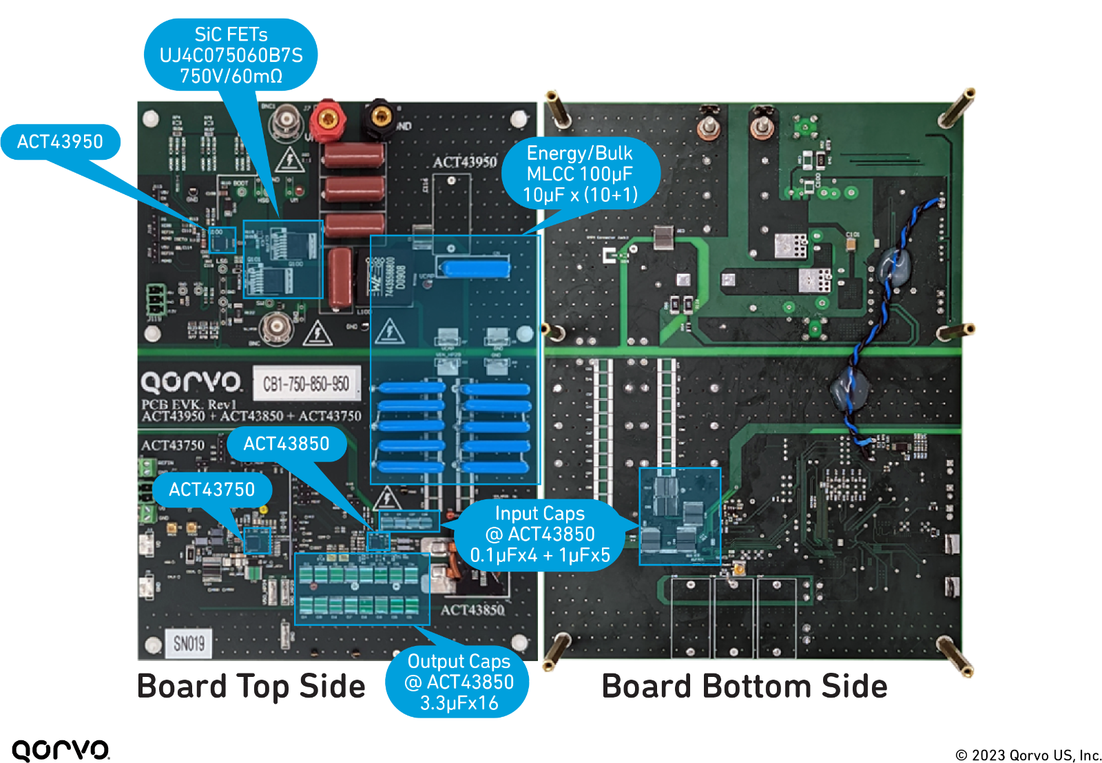
Figure 4: Qorvo's evaluation board solutions for phased array radar.
A Final Word
With this new compact solution using SiC FETs, the PMICs (ACT43950, ACT43850, ACT43750) combined with GaN PAs – a fully developed solution can be achieved with minimal design effort. Using this design from Qorvo provides more advantages than those using a multi-vendor approach. This fully programmable design provides auto-calibration to compensate for temperature changes and aging by constantly self-biasing and monitoring the system, as well as providing automatically optimized powering up and down for the GaN PAs. All of this helps engineers get to market faster with a next-generation bundled solution to create a state-of-the-art phased array radar system.
For more on this topic and solutions for your latest design challenge, visit the Qorvo Design Hub for a rich assortment of videos, blog articles, white papers, tools and more.
For more information on this and other Qorvo phased array radar solutions, please visit Qorvo.com or reach out to Technical Support.
Have another topic that you would like Qorvo experts to cover? Email your suggestions to the Qorvo Blog team and it could be featured in an upcoming post. Please include your contact information in the body of the email.