Thermal Design for Semiconductors and High Power GaN
April 3, 2024
Introduction
Thermal design is a vitally important topic, but sometimes it can seem like a mysterious world of rules, acronyms and equations. But it cannot be ignored: temperature is the biggest environmental reason most semiconductors fail in real-world applications, and every degree rise will reduce a component’s expected lifetime.
In this article, we’ll look at some of the key thermal-related issues design engineers should consider. Specifically, we’ll discuss high-power gallium nitride (GaN) devices and the thermal issues related to their usage.
Thermal Design for Reliability
Thermal design is a complicated subject, but there are some fundamentals that should be explored. Let’s review some basics of using a molded semiconductor on a printed circuit board (PCB).
The first thing to consider is the heat path, which provides a route for heat generated by a semiconductor to the ambient air of the outside world. This heat path should generally go through the bottom of the device package through the ground pad (see Figure 1). Therefore, the application design should incorporate a PCB that pulls the heat from the bottom of the package through the device ground slug.
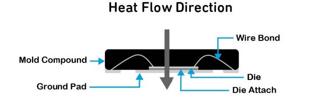
In this type of package, attempting to draw heat from the top of the package will not work due to the poor thermal conductivity of the mold compound, trying to cool it from the top will cause device degradation or failure due to high junction and channel temperatures.
When designing a system or final product, it is important to use as much information and material from the semiconductor vendor as possible, including S2P parameters and PCB Gerber files so that the proper thermal heat extraction methods are employed. For example, placement of via holes and creation of these vias are important to extract heat from your device and increase part reliability – these types of instructions and placements of via holes are generally located in the PCB Gerber files offered by the semiconductor vendor.
Between the ground slug and the PCB will be the solder attach, which should be a high-grade material effective for optimizing thermal dissipation. The via holes’ location, size, and style are typically spelled out by the vendor for optimized performance and should be used with vendor direction. The placement, style, and type of via holes are important to enable a low resistance pathway for the heat. When using a heat sink, attaching it to the lowest impedance path to the IC junction or channel is best.
Additionally, the PCB’s thermal resistance is proportional to the overall thickness of the board – and thermal vias also play a part in this resistance value. Thus, a very thin PCB such as 8-mils is often used for high-power GaN in a quad-flat no-leads (QFN) package to keep the thermal resistance as low as possible. The thermal performance of a PCB material is also dependent on the way the copper is laid out on the board.
To move heat downward to where a heatsink is attached, you will need to use thermal vias at a minimum. These are drilled holes plated with copper to provide thermally conductive pathways from one copper layer to the next. The thicker the copper, the better, as it provides an excellent conductor for heat to dissipate, but the more copper used, the higher the cost.
In lower-power applications, adding layers to the PCB has a big impact on heat conduction away from components. The difference between a two-layer and a four-layer board can be as much as 20°C depending on how well the copper planes are laid out for heat spreading (Figure 2).
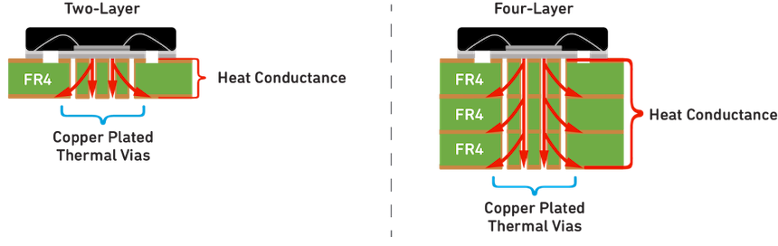
Although adding layers of PCB is a benefit in a low-power situation, doing so in high-power applications has the opposite effect. Adding PCB layers in applications such as GaN high- power devices, especially above 10 to 15 Watts of power, increases resistance and interferes with the heat path.
High-power GaN Application Considerations
For performing thermal analysis of GaN devices and monolithic microwave integrated circuits (MMICs), it is recommended to use an integrated approach that leverages device modeling, empirical measurements (including micro-Raman thermography), and finite element analysis (FEA) simulations. This methodology has proven to be the most effective and accurate. Using this approach, once the baseline thermal model development is completed, FEA is employed to accurately predict channel temperature and themal resistances at the device level.
If micro-Raman thermography and FEA modeling are not an option and only an infrared (IR) camera is available, then the accuracy limitations of IR imaging must be clearly understood. IR cameras have a spatial resolution that is an order of magnitude larger than the gate length of a FET channel and yield area-averaged surface temperatures which are much lower than the true maximum channel temperature.
It is recommended to work closely with the GaN device vendor’s applications teams to ensure the GaN device is operating at a low enough temperature in your application. The applications team can also provide a product bulk thermal model to drop into your system-level thermal model to estimate the device operating environment more accurately, and thus determining the resulting junction or channel temperature.
Improving thermal conductivity in applications
Die only applications
For GaN die components, the die should be mounted directly onto a thermally conductive heat sink material or onto an intermediate carrier plate, for example a die-on-tab. It should be mounted using a gold-tin eutectic solder (preferably) or high thermal conductivity epoxy. The heat sink can be integrated with the next-level assembly, or the die-on-tab can be mounted directly on a heat sink in the next-level assembly using solder or conductive epoxy.
Gold-tin solder and many thermally conductive epoxies have a low thermal resistance value. They also have the ability to accommodate coefficient of thermal expansion (CTE) mismatch stress (often seen when mounting GaN die to high thermal conductivity materials). It is important to ensure the gold-tin solder joint is void-free, especially under the active area of the die. If using a conductive epoxy, the attachment must be uniform and void-free, and have a thin bond line, to maximize thermal conductance.
Mounting a GaN die power device directly onto a PCB is not recommended unless it is mounted to a high-thermal-conductivity coin, for example, a copper coin, to ensure adequate heat transfer.
GaN QFN and surface mount packaged applications
GaN QFN and surface mount packaged components are mounted directly to a PCB. These GaN amplifiers are generally used in intermediate power dissipation applications either in continuous wave (CW) mode or in pulsed applications. In these applications, copper thermal vias are needed to provide a thermally conductive path to the system heat sink. The via size, placement, type, and amount of copper plating should be selected to optimize the overall thermal conductance of the PCB design.
For GaN QFN packages, it is preferred to keep the PCB thickness to a minimum (for example, .008 inches) to keep the thermal resistance low. Using a thin PCB with a dense via array is important, especially for high-frequency GaN MMICs.
Conductive paths are usually the most efficient way to remove heat from a device. For QFN and surface mount packaged amplifiers, having an area-averaged CW heat flux > 1 W/mm 2 out of the bottom of the package is important. Also, using a coined PCB is highly recommended to provide a good thermal path to the system heat sink. Any application above 2 W/mm 2 should definitely have a copper coin under the package.
GaN Copper plated (CP) and flange packaged applications
Providing a good thermal interface between a high-power GaN packaged transistor or packaged MMIC and its heat sink is essential.
Poor package-attach is a major cause of thermal failure. In high-power situations, Qorvo recommends employing a 2 to 4 mils thick (~50-100 µm) thermal interface material (TIM) made from a thermally conductive material (such as indium sheet or graphite film), or a 1 to 2 mils (~25-50 µm) thick layer of thermal grease or thermal compound, covering the entire package base area for mounting flange-based packages.
One thing to note with TIMs is that sufficient pressure is required to obtain good heat transfer. When using a thermal grease or a thermal compound, a minimum of 80% coverage is required.
Conclusions
Good thermal design is essential for reliable operation in the field, particularly for high-power components that generate substantial amounts of heat.
By following best practice thermal design techniques, engineers can ensure they optimize their systems to minimize problems and extend component lifetimes as far as possible.