A Primer on GaN and 3 Reasons It Outperforms Other Semiconductors in RF Applications

April 20, 2017

Gallium (Ga) is a chemical element with atomic number 31. Gallium doesn’t exist freely in nature. Instead, it’s a byproduct in the production of zinc and aluminum.

The GaN compound is formed by gallium and nitrogen atoms arranged, most commonly, in a wurtzite crystal structure. The wurtzite crystal structure (shown in the figure below) is hexagonal and is characterized by two lattice constants (marked a and c in the figure).
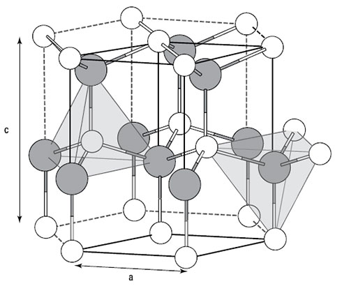
The GaN crystal structure

The GaN crystal structure

In the semiconductor world, GaN is usually grown at a high temperature (approximately 1,100°C) by metal organic chemical vapor deposition (MOCVD) or molecular beam epitaxy (MBE) techniques on a foreign substrate (silicon carbide [SiC] for RF applications, or silicon [Si] for power electronics applications).

The GaN-on-SiC approach combines the high power density capabilities of GaN with the superior thermal conductivity and low RF losses of SiC. That’s why GaN-on-SiC is the combination of choice for high power density RF performance. Today, you can get GaN-on-SiC substrates up to 6 inches in diameter.

The GaN-on-Si combination has a much poorer thermal performance and higher RF losses but is much cheaper. That’s why GaN-on-Si is the combination of choice for price-sensitive power electronics applications. Today you can get GaN-on-Si substrates up to 8 inches in diameter.

So why does GaN outperform other semiconductors in RF applications?

GaN is a relatively new technology compared to other semiconductors, such as Si and GaAs, but it has become the technology of choice for high-RF, power-hungry applications like those required to transmit signals over long distances or at high-end power levels (such as radar, base transceiver stations [BTS], satellite communications, electronic warfare [EW], and so on).

GaN-on-SiC stands out in RF applications for several reasons:

  1. High breakdown field: Because of GaN’s large bandgap, the GaN material has a high breakdown field, which allows the GaN device to operate at much higher voltages than other semiconductor devices. When subjected to high enough electric fields, the electrons in the semiconductor can acquire enough kinetic energy to break the chemical bond (a process called impact ionization or voltage breakdown). If impact ionization is not controlled, it can degrade the device. Because GaN devices can operate at higher voltages, they can be used in higher-power applications.
  2. High saturation velocity: Electrons on GaN have a high saturation velocity (the velocity of electrons at very high electric fields). When combined with the large charge capability, this means that GaN devices can deliver much higher current density.
     
    The RF power output is the product of the voltage and the current swings, so a higher voltage and current density can produce higher RF power in a practically sized transistor. Simply put, GaN devices can produce much higher power density.
  3. Outstanding thermal properties: GaN-on-SiC devices exhibit outstanding thermal properties, due largely to the high thermal conductivity of SiC. In practical terms, this means that GaN-on-SiC devices don’t get as hot as GaAs or Si devices when dissipating the same power. A “colder” device means a more reliable device.

To learn more about GaN, including the benefits of GaN’s high power density, download our e-book, GaN RF Technology For Dummies®.

– Excerpted with permission from John Wiley & Sons, Inc., from GaN RF Technology For Dummies.

GaN For Dummies® Volume 1

Stay up to date with us.

Sign up for notification on new products, product/process change notifications (PCNs) and end of life (EOL) alerts.

Sign Up

Qorvo products are at work connecting, protecting and powering the planet. We bring core radio frequency (RF) and power technologies and solutions to automotive, consumer, defense & aerospace, industrial & enterprise, infrastructure and mobile markets.

Stay Connected

  • Facebook
  • X
  • LinkedIn
  • YouTube
  • Products
  • Solutions
  • Design Hub
  • New Products
  • Product Compliance
  • Blog Posts
  • Events & Trade Shows
  • News Releases
  • Success Stories
  • Technical Articles
  • About Us
  • Careers
  • Corporate Videos
  • Quality
  • Locations
  • Investors
  • How to Buy
  • Forums
  • Portals
  • Contact Us
  • Subscription Center
Site MapFeedbackLegalPrivacySupply Chain Transparency

© 2026 Qorvo US, Inc

|

+1-833-641-3810

A Primer on GaN and 3 Reasons It Outperforms Other Semiconductors in RF Applications

April 20, 2017

Gallium (Ga) is a chemical element with atomic number 31. Gallium doesn’t exist freely in nature. Instead, it’s a byproduct in the production of zinc and aluminum.

The GaN compound is formed by gallium and nitrogen atoms arranged, most commonly, in a wurtzite crystal structure. The wurtzite crystal structure (shown in the figure below) is hexagonal and is characterized by two lattice constants (marked a and c in the figure).

The GaN crystal structure

The GaN crystal structure

In the semiconductor world, GaN is usually grown at a high temperature (approximately 1,100°C) by metal organic chemical vapor deposition (MOCVD) or molecular beam epitaxy (MBE) techniques on a foreign substrate (silicon carbide [SiC] for RF applications, or silicon [Si] for power electronics applications).

The GaN-on-SiC approach combines the high power density capabilities of GaN with the superior thermal conductivity and low RF losses of SiC. That’s why GaN-on-SiC is the combination of choice for high power density RF performance. Today, you can get GaN-on-SiC substrates up to 6 inches in diameter.

The GaN-on-Si combination has a much poorer thermal performance and higher RF losses but is much cheaper. That’s why GaN-on-Si is the combination of choice for price-sensitive power electronics applications. Today you can get GaN-on-Si substrates up to 8 inches in diameter.

So why does GaN outperform other semiconductors in RF applications?

GaN is a relatively new technology compared to other semiconductors, such as Si and GaAs, but it has become the technology of choice for high-RF, power-hungry applications like those required to transmit signals over long distances or at high-end power levels (such as radar, base transceiver stations [BTS], satellite communications, electronic warfare [EW], and so on).

GaN-on-SiC stands out in RF applications for several reasons:

  1. High breakdown field: Because of GaN’s large bandgap, the GaN material has a high breakdown field, which allows the GaN device to operate at much higher voltages than other semiconductor devices. When subjected to high enough electric fields, the electrons in the semiconductor can acquire enough kinetic energy to break the chemical bond (a process called impact ionization or voltage breakdown). If impact ionization is not controlled, it can degrade the device. Because GaN devices can operate at higher voltages, they can be used in higher-power applications.
  2. High saturation velocity: Electrons on GaN have a high saturation velocity (the velocity of electrons at very high electric fields). When combined with the large charge capability, this means that GaN devices can deliver much higher current density.
     
    The RF power output is the product of the voltage and the current swings, so a higher voltage and current density can produce higher RF power in a practically sized transistor. Simply put, GaN devices can produce much higher power density.
  3. Outstanding thermal properties: GaN-on-SiC devices exhibit outstanding thermal properties, due largely to the high thermal conductivity of SiC. In practical terms, this means that GaN-on-SiC devices don’t get as hot as GaAs or Si devices when dissipating the same power. A “colder” device means a more reliable device.

To learn more about GaN, including the benefits of GaN’s high power density, download our e-book, GaN RF Technology For Dummies®.

– Excerpted with permission from John Wiley & Sons, Inc., from GaN RF Technology For Dummies.

GaN For Dummies® Volume 1

Stay up to date with us.

Sign up for notification on new products, product/process change notifications (PCNs) and end of life (EOL) alerts.

Sign Up

Qorvo products are at work connecting, protecting and powering the planet. We bring core radio frequency (RF) and power technologies and solutions to automotive, consumer, defense & aerospace, industrial & enterprise, infrastructure and mobile markets.

Stay Connected

  • Facebook
  • X
  • LinkedIn
  • YouTube
  • Products
  • Solutions
  • Design Hub
  • New Products
  • Product Compliance
  • Blog Posts
  • Events & Trade Shows
  • News Releases
  • Success Stories
  • Technical Articles
  • About Us
  • Careers
  • Corporate Videos
  • Quality
  • Locations
  • Investors
  • How to Buy
  • Forums
  • Portals
  • Contact Us
  • Subscription Center
Site MapFeedbackLegalPrivacySupply Chain Transparency

© 2026 Qorvo US, Inc

|

+1-833-641-3810

Qorvo
  • Products
  • Solutions
  • Design Hub
  • Support
  • About Us
Qorvo
Qorvo
Qorvo
  • Products
  • Solutions
  • Design Hub
  • Support
  • About Us
Qorvo
Qorvo