Wide Bandgap FETs Make Regulating High Voltage Simple
September 8, 2023
Charley Moser, EE Ph.D., was one of my earliest mentors for analog design. While I learned many things from him - hybrid pi transistor modeling, the limitation of Bode plots for stability analysis to minimum phase systems, why use a snubber and how to design one, pulling current of the base of a bipolar to prevent breakdown, SCR use at high temperature - the most strikingly novel was how to regulate low power at high voltage. This was particularly valuable to me because I was the go-to guy for designing the high-voltage power supplies used in charged-particle optics at various instrumentation companies.
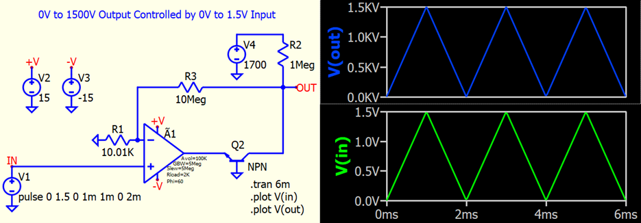
He taught me to use shunt regulation with a grounded-base high-voltage transistor and drive the emitter from an op-amp. The transistor's gain bandwidth would be 3dB down at its fT. Controlling an HV output with a low voltage input entailed a large feedback divider ratio, killing the open loop gain, so the transistor's huge contribution in voltage gain in grounded-base configuration was useful and shouldn't be too hard to tame for a stable loop.
This simulation illustrates the concept:

- Fast: The world's most advanced SPICE engine plus digital (mixed-mode) simulation
- Flexible: No feature limitations
- Free: Free for everyone with no model restrictions
A practical circuit based on everyone's favorite color TV transistor, along with its large signal step response, might look like this:
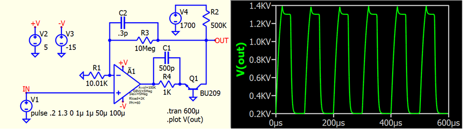
It's a little dicey using the transistor way beyond its open circuit base voltage rating, but grounding the base will bleed off any collector-base leakage and make it as unlikely as possible to break down. The positive rail is reduced to 5V so that the base emitter also won't ever avalanche, which possibly ages the transistor. In adjusting the compensation values, one quickly gets to the point where it's hard to improve settling time.
But today's wide bandgap FETs make the design of such a circuit trivial. There's no need to worry about the voltage rating, and it’s easier to compensate, settling in a fraction of the time of the above design. Plus, there's no need for a negative rail.
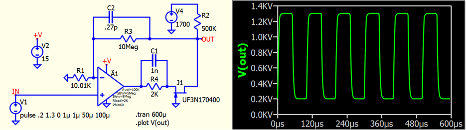
If your cabling to the load is low enough capacitance, you might want an even higher impedance version with a smaller JFET to take advantage of it's reduced capacitance.
I lost touch with Charley about 40 years ago (my bad) but I think he would have liked using a wide bandgap FET.
Additional resources:
Start your own simulation using QSPICE from Qorvo
Have another topic that you would like Qorvo experts to cover? Email your suggestions to the Qorvo Blog team and it could be featured in an upcoming post. Please include your contact information in the body of the email.
