ACT43750
RFPoL (Point of Load) Drain-Switch Driver / Gate-Bias Regulator
Key Features
- State-machine logic:
- Auto-calibration anytime in the field after shipment
- On-PCB RSNS-base, digital ±31% in 1% step program
- RF GaN PA sequencing / protections
- Drain-switch, ON and OFF the pre-regulated DC supply:
- Drain supply input voltage: 10 to 55 V
- TRISE / TFALL: 30 ns (typ)
- Gate-bias regulator:
- Output voltage: -6 to -1.5 V w/ 732 µVSTEP
- Output source current: 300 mA, (peak 500mA)
- Low-noise output: < 200 µVRMS
Typical Applications
- RF GaN / GaAs PA Power Supply
- Military Radar Systems
- Civilian Radar Systems
- Satellite Communications - Uplink
Product Categories
| Pulse Control Mode | Drain |
| Min Drain Switch Voltage(V) | 10 |
| Max Drain Switch Voltage(V) | 55 |
| External Switch FET Support | Power GaN, Power Si |
| Negative Gate Regulator Bias Range(V) | -6 to -1.5 |
| IDQ Auto Calibration | Yes |
| Automatic Power Sequencer | Yes |
| Negative Gate Voltage Generation | Yes |
| Package Type | QFN, 40-pin |
| Package(mm) | 5.0 x 5.0 |
| RoHS | Yes |
| Lead Free | Yes |
| Halogen Free | Yes |
| ITAR Restricted | No |
| ECCN | EAR99 |
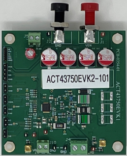 ACT43750EVK3-101 Evaluation Kit
ACT43750EVK3-101 Evaluation Tool User Guide
The Evaluation Tool Users Guide describes the characteristics and operation of the Qorvo ACT43750EVK3-101 evaluation kit (EVK). It provides setup and operation instructions, schematic, layout, BOM, and test data.
To communicate with the EVK, a USB Dongle and a Graphical User Interface (GUI) is provided.
This EVK demonstrates the ACT43750-101 Radar Power IC.
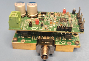 QPA2811PCK01 Reference Design
The QPA2811PCK01 Reference Design provides the user with a QPA2811EVB mated to a Qorvo ACT43750 bias controller PCB.
The QPA2811 a high-power X-band GaN amplifier that covers 8.5 – 10.55 GHz. It provides 48.9 dBm of saturated output power and 27.9 dB of large-signal gain while achieving 48.5 % power-added efficiency. The QPA2811 requires a negative gate bias voltage rail, startup and shutdown sequencing, IDQ calibration, and drain switching circuitry.
The ACT43750 provides the requirements above, plus fault protection and built-in power management that allows the customer to test both boards from a single 24V input.
The Reference Design User Guide describes the characteristics and operation of the QPA2811PCK01 Reference Design. It provides setup and operation instructions, schematic, layout, BOM, and test data.
A Graphical User Interface (GUI) and USB Dongle are provided to communicate with the reference design via I2C from a laptop computer.
This reference design demonstrates both the QPA2811 and the ACT43750 operation.
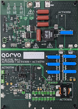 ACT43x50PCKCB1 Evaluation Kit
ACT43x50PCKCB1 Evaluation Tool Users Guide
The Evaluation Tool Users Guide describes the characteristics and operation of the Qorvo ACT43x50PCKCB1 evaluation kit (EVK). It provides setup and operation instructions, schematic, layout, BOM, and test data.
To communicate with the EVK, a USB Dongle and a Graphical User Interface (GUI) is provided.
This EVK demonstrates the ACT43750-101, ACT43850-101, and the ACT43950 Radar Power ICs.
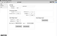 ACT43750 GUI
The ACT43750 Graphical User’s Interface (GUI) is packaged in a ZIP file. This file includes the software, all necessary drivers to communicate with the ACT43750EVK3 Evaluation Tool, and detailed instructions for using the tool.