Quick Guide to High Voltage Impedance Tuning
October 5, 2020

Antenna designers face a multitude of challenges with mobile handsets: the ever-increasing band coverage requirements, challenging industry design constraints, and the continually shrinking amount of real estate left to fit antennas. By using aperture and impedance tuners, designers can tackle these issues. However, not just any aperture or impedance tuner can be used. Many applications today require a more robust, reliable tuning product to fully meet design needs.
Impedance Matching Versus RF Voltage
One challenge designers often grapple with is the RF energy seen on an antenna. For example, impedance matching to an antenna can generate high RF voltage on the matching networks. When matching to impedances that are highly capacitive or inductive, large differential voltages between the matching network and the antenna can occur. This can cause degradation to system performance when lower rated voltage devices are used. To mitigate this degradation, the use of high voltage rated impedance-matching devices is required. Using these types of impedance-matching devices is imperative to withstanding the increased levels of RF voltage. Figure 1 illustrates what level RF voltages can be seen when transmitting at high (GSM850/900) power levels.
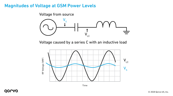 Figure 1.
A Closer Look at Antenna Impedance
Several factors, such as application and antenna design, can affect voltage levels seen on the antenna. Three of those factors include:
- Antenna impedances at the matching device can cause high voltages
- Input power levels in an application (i.e., Power Class 2 (PC2) or GSM)
- Impedances of the actual matching devices
With these three factors in mind, let’s take a closer look at how we use antenna patterns and antenna tuners to optimize our antenna design.
A Deeper Look into Impedance Matching
Impedance matching devices affect power levels and require higher rated voltage level devices to optimize antenna efficiency.
Figure 2 below shows two antenna designs – Pattern A and B. In the following paragraphs, we will describe how these patterns interact with impedance matching components of differing voltage ratings. We will also show how the higher rated device helps maximize total radiated efficiency.
 Figure 2.
To begin, in Figure 3 below, we see how the antenna pattern “A” and “B” measure on a Smith Chart over low band GSM frequencies. As shown, the antenna impedance lies in the inductive region of the Smith Chart, making a series capacitor an optimal matching solution. Thus, our antenna matching solution will use a capacitor.
 Figure 3.
In our example, two similar devices shown in Figure 4 to the left were measured and compared as impedance matching applications to the antenna. One was rated for 55VRF (DEVICE55) and the other for 65VRF (DEVICE65). Each device is comprised of a programmable capacitor capable of 32 unique states of capacitance, as well as an independent toggleable switch.
 Figure 4.
The state of each device was selected to maximize radiated efficiency of Antenna Pattern A across the low-band frequency realm. Additionally, the device states were chosen to adhere to the rated RF voltages for each device: 55VRF for DEVICE55 and 65VRF for DEVICE65, as shown in the figure below. The devices were tested at GSM850/900 as well as LTE B12 (Band 12). The measurement chart (Figure 5) below illustrates an efficiency vs frequency plot of the antenna interfaced with these two devices.
 Figure 5.
The output measurement above utilizes antenna pattern “A” for both DEVICE 55 and DEVICE 65. As shown, the efficiency suffers greatly in the GSM850 and GSM900 Tx frequencies if the lower 55 volt device is used. To achieve better efficiency across GSM850, GSM900 and B12 while maintaining voltages, the voltage of DEVICE65 should be selected, as the efficiency exceeds that of DEVICE55.
To improve the DEVICE55 response, we attempted to use pattern “B” antenna design. The output measurement chart below shows pattern “A” using DEVICE65. For DEVICE55 we used pattern “B”. Although DEVICE55 does improve using the pattern “B” antenna design in GSM frequencies, it still does not improve enough to meet the DEVICE65 component. As shown in Figure 6, DEVICE65 efficiency once again exceeds that of DEVICE55. This is attributed to DEVICE65’s ability to meet the higher RF voltage input impedance.
 Figure 6.
Additionally, utilizing pattern “B”, the efficiency using DEVICE55 is not as high or as broadband as pattern “A” paired with DEVICE65, particularly at the B12 frequency range. Although DEVICE55 did show some improvement using pattern “B” the DEVICE55 was not as efficient as pattern “A” with DEVICE65.
In summary, the higher voltage seen on the antenna does affect efficiency and performance. Our measurements confirmed that the higher rated voltage devices allow more capability when used in impedance matching applications with high RF voltage. In our example, we utilized two Qorvo configurable tuners, each compromised of a switch and programmable array of capacitors (PAC), with one device rated for 55Vp and the other rated for 65Vp. The higher rated component provides more margin for antenna designers. In turn, this allows system designers to match circuits more effectively to multiple antenna patterns and RF voltage scenarios, without modifying the design layout structure.
Have another topic that you would like Qorvo experts to cover? Email your suggestions to the Qorvo Blog team and it could be featured in an upcoming post. Please include your contact information in the body of the email.