QPA2811
X-Band 60 Watt GaN Power Amplifier
Recommended driver amplifier: QPA0812
Key Features
- Frequency Range: 8.5 - 10.55 GHz
- PSAT (PIN=21 dBm): 48.9 dBm
- PAE (PIN=21 dBm): 48.5 %
- Power Gain (PIN=21 dBm): 27.9 dB
- Bias: VD = 24 V, IDQ = 1.24 A
- Package Dimensions: 7.0 x 7.0 x 0.82 mm
Qorvo's QPA2811 is a packaged, high-power X-band amplifier fabricated on Qorvo’s production 0.15 um GaN on SiC process (QGaN15). Covering 8.5 - 10.55 GHz, the QPA2811 provides 48.9 dBm of saturated output power and 27.9 dB of large-signal gain while achieving 48.5 % power-added efficiency.
The QPA2811 is packaged in a 7 mm x 7 mm 48-pin plastic overmolded package. It can support a variety of operating conditions to best support system requirements. With good thermal properties, it can support a range of bias voltages.
The QPA2811 MMIC RF ports are DC grounded and matched to 50 ohms. The QPA2811 is ideal for military radar systems.
Lead-free and RoHS compliant.
Typical Applications
- Radar
Product Categories
Application Categories
| Frequency Min(GHz) | 8.5 |
| Frequency Max(GHz) | 10.55 |
| Pout(dBm) | 49 |
| Psat(dBm) | 48.9 |
| Gain(dB) | 27.9 |
| PAE(%) | 48.5 |
| Voltage(V) | 24 |
| Current(mA) | 1.24 |
| Package Type | QFN Overmold |
| Package(mm) | 7.0 x 7.0 x 0.82 |
| RoHS | Yes |
| Lead Free | Yes |
| Halogen Free | Yes |
| ITAR Restricted | No |
| ECCN | 3A001.B.2.B.2 |
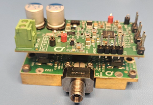 QPA2811PCK01 Reference Design
The QPA2811PCK01 Reference Design provides the user with a QPA2811EVB mated to a Qorvo ACT43750 bias controller PCB.
The QPA2811 a high-power X-band GaN amplifier that covers 8.5 – 10.55 GHz. It provides 48.9 dBm of saturated output power and 27.9 dB of large-signal gain while achieving 48.5 % power-added efficiency. The QPA2811 requires a negative gate bias voltage rail, startup and shutdown sequencing, IDQ calibration, and drain switching circuitry.
The ACT43750 provides the requirements above, plus fault protection and built-in power management that allows the customer to test both boards from a single 24V input.
The Reference Design User Guide describes the characteristics and operation of the QPA2811PCK01 Reference Design. It provides setup and operation instructions, schematic, layout, BOM, and test data.
A Graphical User Interface (GUI) and USB Dongle are provided to communicate with the reference design via I2C from a laptop computer.
This reference design demonstrates both the QPA2811 and the ACT43750 operation.
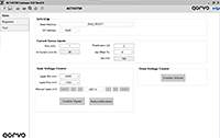 ACT43750 GUI
The ACT43750 Graphical User’s Interface (GUI) is packaged in a ZIP file. This file includes the software, all necessary drivers to communicate with the ACT43750EVK3 Evaluation Tool, and detailed instructions for using the tool.